ELECTRICITY
The topics covered are:
- monitoring and measuring AC
- current, potential difference, power, and resistance
- electrical sources and internal resistance
- capacitors
- semiconductors and p-n junctions

|
|
SUB UNIT HEADING |
DETAILS |
|
Monitoring and measuring AC
|
- Knowledge that AC is a current which changes direction and instantaneous value with time.
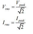
- Use of appropriate relationships to solve problems involving root mean square (rms) and peak values. 
- Determination of frequency, peak and rms values from graphical data.
Vertical Divider
|
|
Current, potential difference, power, and resistance
|
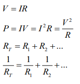
- Use of appropriate relationships to solve problems involving potential difference, current, power, and resistance. Solutions may involve several steps.
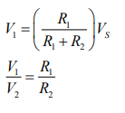
- Use of appropriate relationships to solve problems involving potential divider circuits.
Vertical Divider
|
|
Electrical sources and internal resistance
|

- Knowledge of the terms electromotive force (EMF), internal resistance, lost volts, terminal potential difference (t.p.d.), ideal supplies, short circuit and open circuit.
- Use of appropriate relationships to solve problems involving EMF, lost volts, t.p.d., current, external resistance, and internal resistance. - Description of an experiment to measure the EMF and internal resistance of a cell. - Determination of EMF, internal resistance and short circuit current using graphical analysis. Vertical Divider
|
|
Capacitors
|

- Knowledge that a capacitor of 1 farad will store 1 coulomb of charge when the potential difference across it is 1 volt.
- Use of an appropriate relationship to solve problems involving capacitance, charge and potential difference. 
- Use of an appropriate relationship to determine the charge stored on a capacitor for a constant charging current.
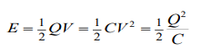
- Knowledge that the total energy stored in a charged capacitor is equal to the area under a charge potential difference graph.
- Use of appropriate relationships to solve problems involving energy, charge, capacitance, and potential difference. - Knowledge of the variation of current and potential difference with time for both charging and discharging cycles of a capacitor in an RC circuit (charging and discharging curves). - Knowledge of the effect of resistance and capacitance on charging and discharging curves in an RC circuit. - Description of experiments to investigate the variation of current in a capacitor and voltage across a capacitor with time, for the charging and discharging of capacitors. Vertical Divider
|
|
Semiconductors and p-n junctions
|
- Knowledge of the terms conduction band and valence band.
- Knowledge that solids can be categorised into conductors, semiconductors or insulators by their band structure and their ability to conduct electricity. Every solid has its own characteristic energy band structure. For a solid to be conductive, both free electrons and accessible empty states must be available. - Qualitative explanation of the electrical properties of conductors, insulators and semiconductors using the electron population of the conduction and valence bands and the energy difference between the conduction and valence bands. (Reference to Fermi levels is not required.) - The electrons in atoms are contained in energy levels. When the atoms come together to form solids, the electrons then become contained in energy bands separated by gaps. - For metals we have the situation where one or more bands are partially filled. Some metals have free electrons and partially filled valence bands, therefore they are highly conductive. Some metals have overlapping valence and conduction bands. Each band is partially filled and therefore they are conductive. - In an insulator, the highest occupied band (called the valence band) is full. The first unfilled band above the valence band is the conduction band. For an insulator, the gap between the valence band and the conduction band is large and at room temperature there is not enough energy available to move electrons from the valence band into the conduction band where they would be able to contribute to conduction. There is no electrical conduction in an insulator. - In a semiconductor, the gap between the valence band and conduction band is smaller and at room temperature there is sufficient energy available to move some electrons from the valence band into the conduction band allowing some conduction to take place. An increase in temperature increases the conductivity of a semiconductor. - Knowledge that, during manufacture, semiconductors may be doped with specific impurities to increase their conductivity, resulting in two types of semiconductor: p-type and n-type. - Knowledge that, when a semiconductor contains the two types of doping (p-type and ntype) in adjacent layers, a p-n junction is formed. There is an electric field in the p-n junction. The electrical properties of this p-n junction are used in a number of devices. - Knowledge of the terms forward bias and reverse bias. Forward bias reduces the electric field; reverse bias increases the electric field in the p-n junction. - Knowledge that LEDs are forward biased p-n junction diodes that emit photons. The forward bias potential difference across the junction causes electrons to move from the conduction band of the n-type semiconductor towards the conduction band of the ptype semiconductor. Photons are emitted when electrons ‘fall’ from the conduction band into the valence band either side of the junction. - Knowledge that solar cells are p-n junctions designed so that a potential difference is produced when photons are absorbed. (This is known as the photovoltaic effect.) The absorption of photons provides energy to ‘raise’ electrons from the valence band of the semiconductor to the conduction band. The p-n junction causes the electrons in the conduction band to move towards the n-type semiconductor and a potential difference is produced across the solar cell. Vertical Divider
|
Summary Notes & Questions
Remember to continual check your past paper attempts and review unknown areas with your summary notes. Websites like BBC Bitesize and Mr MacKenzie Fizzics will also help your revision. Ask your teacher if you are unsure of how to proceed with your revision plan and to clarify areas you are unsure about.
